Design of Wilkinson RF Power Divider
For any beginner in RF circuit design, 2way hybrid design is the first step to get familiar with the concepts of rf circuit design right from simulation, tuning, optimization and layout using RF design softwares. The most popular softwares are microwave office and ADS. In this page we will go through wilkinson 2-way RF splitter design at

1 to 18GHz 4-way Power Divider
800MHz using dielectric substrate having εr of 4.6. The same design can be extended for N-Way power divider or splitter such as 8-WAY and 16-WAY. This higher number of ports rf combiner and splitter is widely used in VSAT Hub stations or central stations for multiple signal combining and splitting process.

Wilkinson power divider is the robust among all designs. It will have all the output ports matched. It will have only reflected power which will be dissipated. It provides better isolation between output ports in comparison to T-junction power divider. Figure above mentions both geometry layout as well as transmission line equivalent circuit of the power splitter.
RF Simulation Circuit

The figure depicts wilkinson 2way power splitter circuit used for simulation using Microwave Office software. Simulate the rf circuit from frequency 500 to 1100 MHz and check the results as shown. Set the microstrip substrate parameters as shown in the table below in the simulation circuit.
| Substrate Specifications | Value |
|---|---|
| Relative Dielectric Constant(εr) | 4.6 |
| Substrate thickness(H) | 1.6 mm |
| Conductor thickness(T) | 0.05 mm |
| Rho(Metal Bulk resistivity normalized to gold) | 1 |
| Tand(Loss tangent of dielectric) | 0.025 |
| Dielectric material | GaAs |
Results
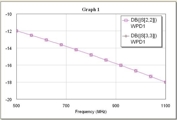
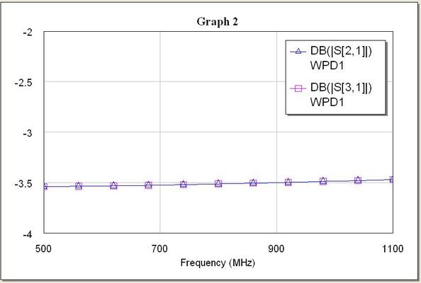
The figure depicts results of our design. As mentioned S11, S22, S33 are better than -15dB. S21 and S31 are better than about -3dB.
Layout schematic
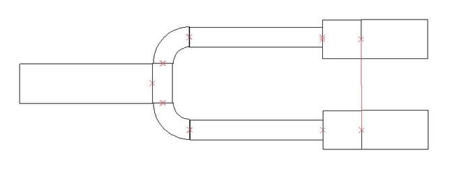
The figure depicts final layout of 2way rf power splitter as per wilkinson design concepts mentioned. After the basic layout is generated, the same is modified as per PCB requirement and placement of RF connectors. The mounting of chip resistors of value 50 Ohm and 100 Ohm is also made manually. Refer microstrip line basics and types which will help rf designer to understand concepts before RF circuit design as mentioned in this example.
-
 6-18GHz 4-way Stripline Power Divider,PD00566
 -
 6-10GHz 4-way Stripline Power Divider,PD00371
 -
 8-12.4GHz 2-way Stripline Power Divider,PD00372
 -
 2-6GHz 4-way Stripline Power Divider,PD00554
 -
 0.5-18GHz 4-way Stripline Power Divider,PD00315
 -
 0.5-18GHz 2-way Stripline Power Divider,PD00508
 -
 19.2-21.2GHz 2-way Stripline Power Divider,PD00506
 -
 17-40GHz 2-way Stripline Power Divider,PD00504
 -
 1-18GHz 4-way Stripline Power Divider,PC00006
 -
 0.5-2GHz 2-way Stripline Power Divider,PD00519
 -
 DC-40GHz 2-way Resistive Power Divider,PD00548
 -
 6-18GHz 4-way Stripline Power Divider,PD00252


-
6-18GHz 4-way Stripline Power Divider,PD00566
-
6-10GHz 4-way Stripline Power Divider,PD00371
-
8-12.4GHz 2-way Stripline Power Divider,PD00372
-
2-6GHz 4-way Stripline Power Divider,PD00554
-
0.5-18GHz 4-way Stripline Power Divider,PD00315
-
0.5-18GHz 2-way Stripline Power Divider,PD00508
-
 DC-0.36GHz Suspended Stripline Low Pass Filter,F00715
 -
 DC-5GHz Suspended Stripline Low Pass Filter,F00471
 -
 32-40GHz Cavity Band Pass Filter,F00744
 -
 31-40GHz Cavity Band Pass Filter,F00745
 -
 29-34GHz Cavity Band Pass Filter,F00742
 -
 27-40GHz Cavity Band Pass Filter,F00743


Related Posts
No Image
Newsletter – 2103 – Panda Microwave
2021年3月24日
Panda Microwave RF & Microwave components suppler…Read more
No Image
Wilkinson Power Divider, Splitter & Combiner
2020年5月13日
Wilkinson Power Divider, Splitter & Combiner From https://www.electronics-notes.com/ The Wilkinson configuration is a very effective…Read more
No Image
Wilkinson power divider Theory
2020年5月13日
From Wikipedia, the free encyclopedia Power divider in microstrip technology In the field of microwave engineering…Read more
No Image
What differentiates a power splitter and power divider
2020年5月12日
The fundamental difference between power splitters and power dividers (combiners) is the resistor configuration used…Read more

0.15-3.2GHz 8-way Power Divider Test Curve
2019年6月14日
50 Ohm 8-way SMA-Female Power Divider From 0.15 to 3.2 GHz Rated_At 30 Watts, …Read more

20-25GHz 4-way Power Divider Test Curve
2019年3月30日
50 Ohm 4-way SMA-Female Power Divider From 20 to 25 GHz Rated_At 20 Watts, P…Read more